CMOS Analog and Mixed Signal Circuit Design Practices and Innovations 1st edition by Arjuna Marzuki ISBN 1000071510 978-1000071511
$50.00 Original price was: $50.00.$25.00Current price is: $25.00.
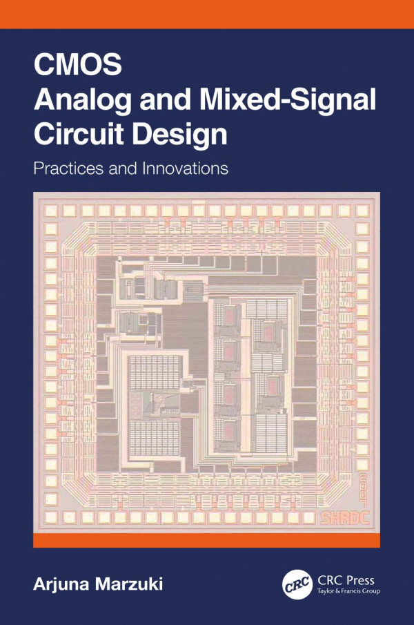
CMOS Analog and Mixed Signal Circuit Design Practices and Innovations 1st edition by Arjuna Marzuki – Ebook PDF Instant Download/Delivery: 1000071510, 978-1000071511
Full download CMOS Analog and Mixed Signal Circuit Design Practices and Innovations 1st Edition after payment
Product details:
ISBN 10: 1000071510
ISBN 13: 978-1000071511
Author: Arjuna Marzuki
The purpose of this book is to provide a complete working knowledge of the Complementary Metal-Oxide Semiconductor (CMOS) analog and mixed-signal circuit design, which can be applied for System on Chip (SOC) or Application-Specific Standard Product (ASSP) development. It begins with an introduction to the CMOS analog and mixed-signal circuit design with further coverage of basic devices, such as the Metal-Oxide Semiconductor Field-Effect Transistor (MOSFET) with both long- and short-channel operations, photo devices, fitting ratio, etc. Seven chapters focus on the CMOS analog and mixed-signal circuit design of amplifiers, low power amplifiers, voltage regulator-reference, data converters, dynamic analog circuits, color and image sensors, and peripheral (oscillators and Input/Output [I/O]) circuits, and Integrated Circuit (IC) layout and packaging.
Features:
Provides practical knowledge of CMOS analog and mixed-signal circuit design
Includes recent research in CMOS color and image sensor technology
Discusses sub-blocks of typical analog and mixed-signal IC products
Illustrates several design examples of analog circuits together with layout
Describes integrating based CMOS color circuit
CMOS Analog and Mixed Signal Circuit Design Practices and Innovations 1st Table of contents:
Chapter 1: CMOS Analog and Mixed-Signal Circuit Design: An Overview
1.1 Introduction
1.2 Notation, Symbol, and Terminology
1.3 Technology, Circuit Topology, and Methodology
1.4 Analog and Mixed-Signal Integrated Design Concepts
1.5 Summary
Chapter 2: Devices: An Overview
2.1 Introduction
2.2 The PN Junction
- 2.2.1 Fermi Level
- 2.2.2 Depletion Layer Capacitance
- 2.2.3 Storage Capacitance
2.3 Photo Devices
2.4 FETs - 2.4.1 Long Channel Approximation
- 2.4.1.1 MOS Structure
- 2.4.1.2 MOS with External Bias
- 2.4.1.3 MOS Operation
- 2.4.1.4 Current-Voltage Characteristics
- 2.4.2 MOSFET Scaling
- 2.4.2.1 Full Scaling
- 2.4.2.2 Constant-Voltage Scaling
- 2.4.3 Weak Inversion
- 2.4.4 Short-Channel
- 2.4.4.1 Carrier Drift Velocity Models
- 2.4.4.2 VDSAT
- 2.4.4.3 Current-Voltage Equation for Short Channel Transistor
- 2.4.5 MOSFET Capacitor
- 2.4.5.1 Oxide-Related Capacitance
- 2.4.5.2 Junction Capacitance
- 2.4.6 MOSFET Transition Frequency
- 2.4.7 Noise
- 2.4.7.1 Thermal Noise
- 2.4.7.2 Flicker Noise
2.5 Process Fitting Ratio
- 2.5.1 150-90 nm Design Transfer
2.6 MOSFET Parameter Exercise
2.7 SPICE Example
2.8 Summary
References
Chapter 3: Amplifiers
3.1 Introduction
- 3.1.1 CMOS Amplifier
3.2 Input Voltage Range - 3.2.1 Theory
- 3.2.2 Example
3.3 Signal Path of CMOS Operational Amplifier - 3.3.1 Overall Signal Path
- 3.3.2 Load
- 3.3.3 Cascode Current Source
- 3.3.4 Example
3.4 CMOS Amplifier Parameters - 3.4.1 Input Offset
- 3.4.2 Common Mode Input Voltage Range
- 3.4.3 Current Consumption
- 3.4.4 Common Mode Rejection Ratio (CMRR)
- 3.4.5 Power Supply Rejection Ratio
- 3.4.6 Slew Rate and Settling Time
- 3.4.7 DC Gain, fc, and fT
- 3.4.8 Noise
- 3.4.9 Distortion
3.5 Common Mode Feedback
3.6 Compensation in Amplifier - 3.6.1 Loop Response
- 3.6.2 Pulse Response
3.7 Wideband Amplifier Technique - 3.7.1 Source and Load
- 3.7.2 Stages and Feedback
3.8 Noise in Amplifiers - 3.8.1 Noise in Circuits
- 3.8.2 Noise in Single-Stage Amplifiers
- 3.8.3 Noise in Differential Pairs
- 3.8.4 Noise in Amplifier with Resistors in the Feedback
- 3.8.5 Noise Bandwidth
3.9 Current Density Design Approach
3.10 Layout Examples
3.11 Summary
References
Chapter 4: Low Power Amplifier
4.1 Introduction
4.2 Low Voltage CMOS Amplifier
- 4.2.1 Body or Bulk Control
- 4.2.2 Circuit Technique
4.3 Subthreshold
4.4 Current Reuse CMOS Amplifier
4.5 Other Techniques - 4.5.1 Common-Gate with Gain-Boosting Wideband Differential LNA
4.6 SPICE Example
4.7 Summary
References
Chapter 5: Voltage Regulator, References and Biasing
5.1 Introduction
5.2 Current Sources
5.3 Self-Biased
5.4 CTAT and PTAT
5.5 Bandgap Voltage Reference
- 5.5.1 Bandgap Reference
5.6 Diode-Less Voltage Reference
5.7 Cascode Current Source
5.8 Regulated Power Supply
5.9 Design Example
5.10 SPICE Example
5.11 Layout Example
5.12 Summary
Problems
References
Chapter 6: Introduction of Advanced Analog Circuit
6.1 Introduction
6.2 MOSFET as a Switch
6.3 Basic Switched Capacitor
- 6.3.1 Switching Capacitor Sensitive to Parasitic Capacitances
6.4 Active Integrator - 6.4.1 Non-inverting Switching Capacitor Non-sensitive to Parasitic Capacitances
- 6.4.2 Inverting Active Integrator without a Delay
- 6.4.3 Inverting the Switching Capacitor with a Delay, Non-sensitive to Parasitic Capacitances
- 6.4.4 SC Behavior in Discrete Points of Time
- 6.4.5 Non-inverting Active Integrator with a Delay
6.5 Sample-and-Hold Amplifier
6.6 Programmable Gain Amplifier - 6.6.1 Timing
- 6.6.2 Common Mode Feedback
- 6.6.2.1 AMP and CMFB
6.7 Chopper Amplifier
6.8 Dynamic Element Matching Technique
6.9 Resistor-Less Current Reference
6.10 Switch Mode Converter
6.11 SPICE Example
6.12 Layout Issue
6.13 Summary
References
- 6.6.2.1 AMP and CMFB
Chapter 7: Data Converter
7.1 Introduction
7.2 Digital-to-Analog Converter
- 7.2.1 Resistor String Topology
- 7.2.2 Current Steering
- 7.2.3 Hybrid Topology
- 7.2.4 DAC Trimming or Calibration
- 7.2.5 Glitch
7.3 Analog-to-Digital Converter - 7.3.1 Slope ADC
- 7.3.2 SAR ADC
- 7.3.3 Flash ADC
- 7.3.4 Pipelined ADC
- 7.3.5 Delta Sigma ADC
7.4 SPICE Example - 7.4.1 DAC Example
- 7.4.2 ADC Example
7.5 Layout Examples
7.6 Summary
References
Chapter 8: CMOS Color and Image Sensor Circuit Design
8.1 Introduction
8.2 Technology and Methodology
- 8.2.1 General Comments on Technology or Process for CMOS Image Sensor
- 8.2.2 Backside Illumination
- 8.2.3 Photo Devices
- 8.2.4 Design Methodology
8.3 CMOS Color Sensor - 8.3.1 Transimpedance Amplifier Topology
- 8.3.2 Current to Frequency Topology
- 8.3.3 Current Integration Topology
8.4 CMOS Image Sensor - 8.4.1 CMOS Image Sensor Architecture
- 8.4.1.1 Pixel-Level ADC
- 8.4.1.2 Column-Level ADC
- 8.4.1.3 Chip-Level ADC
- 8.4.2 Analog Pixel Sensor
- 8.4.3 Digital Pixel Sensor
- 8.4.4 Low Power and Low Noise Technique
- 8.4.4.1 Low Power Techniques
- 8.4.4.2 Low Noise Techniques
8.5 SPICE Example
8.6 Layout
8.7 Summary
References
Chapter 9: Peripheral Circuits
9.1 Introduction
9.2 Oscillator
- 9.2.1 Ring Oscillator
- 9.2.2 RC Oscillator
- 9.2.2.1 Ramp Oscillator
9.3 Non-overlapping Generator
9.4 Interface Circuitry
- 9.2.2.1 Ramp Oscillator
- 9.4.1 Basic Interface Circuit
- 9.4.2 I2C
9.5 I/O Pad
9.6 Schmitt Trigger Circuit
9.7 Voltage Level Shifters
9.8 Power on Reset
9.9 ESD Circuit
9.10 SPICE Example
9.11 Layout Example
9.12 Summary
References
Chapter 10: Layout and Packaging
10.1 Introduction
10.2 Process
- 10.2.1 Antenna Rule
- 10.2.2 Electromigration and Metal Density
- 10.2.3 Shear Stress
10.3 Floor Planning
10.4 ESD and I/O Pad Layout - 10.4.1 Low Parasitic Capacitance Pad
- 10.4.2 Seal Ring
10.5 Analog Circuit Layout Technique - 10.5.1 Matching
- 10.5.2 Guard Ring
- 10.5.3 Shielding
- 10.5.4 Voltage (IR) Drop
- 10.5.5 Metal over Implant
- 10.5.6 Substrate Tap
10.6 Digital Circuit Layout Technique - 10.6.1 Power Distribution for Mixed-Signal Design
- 10.6.2 Clock Distribution
- 10.6.3 Latch-up
10.7 Packaging - 10.7.1 Die Attach
- 10.7.2 Package Type
- 10.7.3 Package Parasitic
10.8 Summary
People also search for CMOS Analog and Mixed Signal Circuit Design Practices and Innovations 1st:
cmos analog and mixed-signal circuit design practices and innovations
analog and mixed signal circuits in nanoscale cmos
what is analog mixed signal design
6.775 cmos analog and mixed signal circuit design
mixed signals in electronics
Tags:
Arjuna Marzuki,CMOS,Analog,Mixed Signal,Circuit,Design,Practices,Innovations 1st
You may also like…
Engineering
Design of CMOS phase locked loops from circuit level to architecture level 1st Edition Behzad Razavi
Engineering - Electrical & Electronic Engineering
Design of Analog CMOS Integrated Circuits 2nd eddition 2nd Edition Behzad Razavi
Technique - Electronics: Signal Processing
Injection-Locking in Mixed-Mode Signal Processing Fei 303017364X 9783030173647


